
Agentic AI for Chip Design: How AWS and ChipAgents Tackle the Engineering Bottleneck

Based on a transcription of Jhen-Wei Huang’s presentation, “AI-Accelerated Chip Design Workflows on AWS.”
Why is chip design so hard to scale?
Chip design remains one of the highest-barrier areas in computing.
A complex semiconductor project can take around 30 months from start to finish. Verification alone can consume a very large share of the total engineering effort. At the same time, advanced projects require massive amounts of compute and storage, expensive EDA licenses, and highly specialized engineering talent.
And that last point is becoming increasingly important.
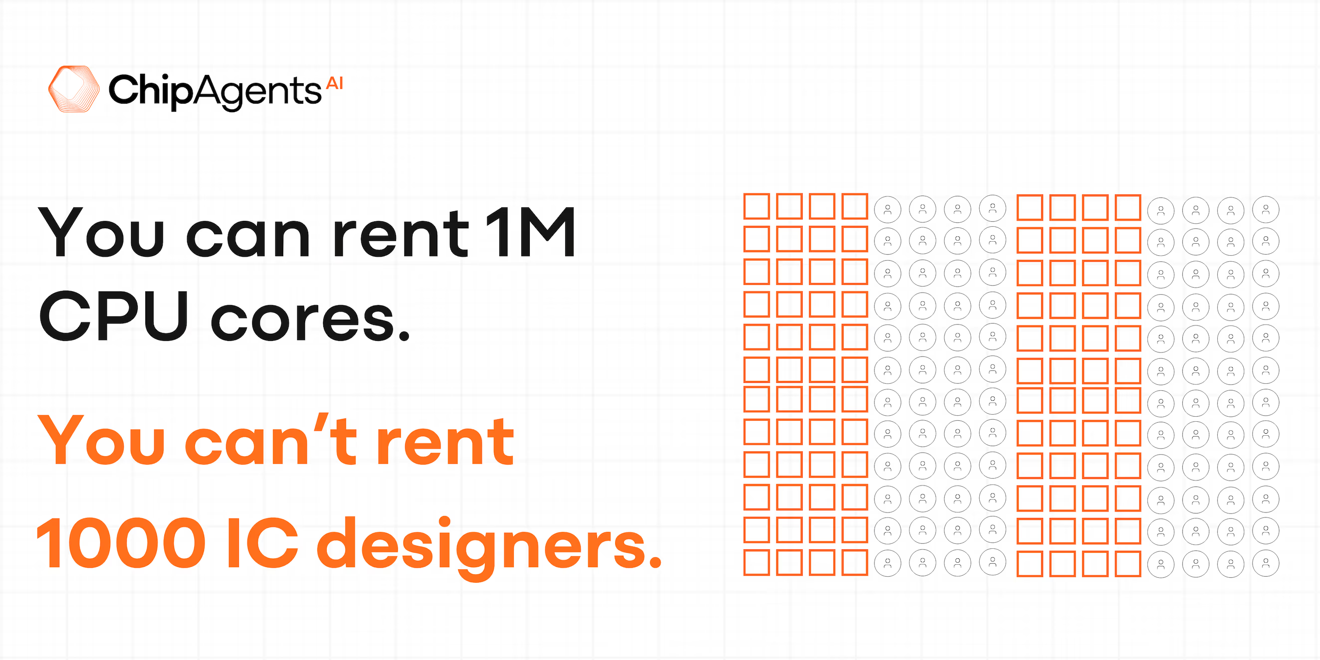
You can rent a million CPU cores.
You cannot rent a thousand experienced IC designers.
That combination of long design cycles, infrastructure requirements, tool costs, and limited engineering talent is why chip design continues to be so difficult to scale.
What infrastructure challenges slow down semiconductor design?
The first challenge is scalability. Before cloud infrastructure became widely adopted for semiconductor design, companies largely had to build and operate their own data centers.
That meant taking responsibility for security, reliability, operational excellence, performance efficiency, cost optimization, and sustainability. Security is particularly important because the core IP of a semiconductor company is its design data. RTL, PDKs, netlists, project data, and other design assets need to be protected throughout the development process. In an on-premises environment, companies have historically had to build and manage that security architecture themselves.
Reliability creates another challenge. If a compute farm experiences a failure shortly before tapeout, there may be no room in the schedule to recover. Building a second data center for disaster recovery is expensive, and design timelines do not stop while infrastructure problems are being fixed.
The third challenge is operational burden. CAD teams also have to manage more than the design tools themselves. They need to install and maintain infrastructure, optimize compute farms, manage storage, define access policies, and make capacity-planning decisions years in advance.
The last challenge is performance. The right compute architecture can directly affect EDA runtime and therefore license efficiency. And because semiconductor workloads have large peaks and valleys, buying enough hardware for peak demand often means leaving significant infrastructure underutilized at other times.
For many years, these burdens were simply considered part of the cost of being a semiconductor company.
Why is engineering talent the biggest bottleneck in chip design?
Cloud infrastructure can provide enormous amounts of compute scaling.
It can provide storage.
It can improve reliability.
It can make infrastructure more elastic.
But it does not automatically create more experienced IC designers.
Design efficiency and quality still depend heavily on engineering expertise.
Experienced engineers know how to reduce trial-and-error cycles, improve first-silicon quality, reduce ECOs, and move projects toward tapeout faster.
At the same time, the semiconductor talent pipeline is under pressure. As the presentation highlighted, one in three U.S. chip engineers is over 55.
That raises a larger question:
If computing resources can now scale almost instantly, can engineering capacity begin to scale in a similar way?
Where can generative AI be used in the semiconductor lifecycle?
Since 2023, AI models have become significantly more capable.
Across financial services, healthcare, automotive, manufacturing, legal workflows, and software engineering, models are increasingly being used for specialized professional tasks rather than only general-purpose assistance.
Software engineering is one of the clearest examples.
AI systems can now generate code, analyze repositories, debug issues, and participate in increasingly complex development workflows.
The natural question is what happens when the same transition reaches hardware design.
Semiconductor development already contains a broad range of possible generative AI use cases.
On the front end, AI can support design planning, testbench generation, RTL generation, intelligent bug triage, design assistance, and log analysis.
In backend verification and implementation, it can support conversational interaction with EDA tools, Perl and Tcl generation, code translation, bug triage, PDK interaction, and other engineering tasks.
Production and test create additional opportunities, including packaging design, test diagnostics, operating-procedure assistance, and equipment fault root-cause analysis.
In other words, AI is not limited to one phase of the semiconductor lifecycle.
Nearly every phase presents potential use cases.
How does AWS support secure AI workloads for chip design?
To support those workloads, AWS has expanded beyond compute and storage infrastructure.
Amazon Bedrock provides access to multiple frontier models through a common service, allowing customers to select different models depending on the task, performance requirements, and budget.
That choice matters because different engineering tasks may benefit from different models.
The model used for coding may not be the same model used for retrieval or reasoning over documentation. As model capabilities evolve, companies also want the ability to change models without rebuilding their entire infrastructure.
Most importantly for semiconductor companies, these AI workloads can remain inside the customer's private environment.
Models, agents, RTL, PDKs, netlists, and other sensitive data can operate inside the customer's VPC, connected privately to existing corporate infrastructure.
That means the same security model previously established for EDA workloads can now extend to the AI layer.
How is agentic AI different from AI built into EDA tools?
Traditional EDA vendors are already incorporating AI and machine learning into their tools.
AI-assisted verification closure, regression selection, synthesis optimization, and design-space exploration are all becoming part of modern EDA workflows.
Those capabilities can provide real productivity improvements.
But they often remain tied to individual point tools.
The engineer still has to connect the steps across the overall design flow.
Agentic AI introduces a different possibility.
Instead of applying AI only within one EDA application, specialized agents can work across tasks and tools.
That is where ChipAgents enters the picture.
ChipAgents provides agentic AI built specifically for semiconductor design and verification, including workflows such as specification-to-RTL generation, test generation, simulation orchestration, and autonomous bug hunting.
The larger goal is to give semiconductor organizations something cloud infrastructure by itself cannot provide: experienced design capacity on demand.
How do multiple AI agents work together across a chip-design flow?

The next step is to move beyond individual agents.
A full chip-design workflow requires multiple engineering disciplines.
There may be separate agents for design verification, synthesis, timing, place-and-route, CFD, simulation, and reporting.
Those agents need coordination.
One approach is to use a principal or supervisor agent that understands the overall engineering objective and dispatches tasks to specialized domain agents.
For example, a principal agent might receive a high-level design request, break it into tasks, and coordinate individual agents responsible for verification, synthesis, timing, P&R, and other steps.
The underlying models can also vary.
One model might be used as the primary reasoning system, another as a fallback, and still another for specific tool-oriented tasks.
The important point is that the role itself is assembled dynamically from the agents and tools required for the job.
How do you keep autonomous AI agents under control in chip design?
An autonomous engineering environment cannot simply allow models to act without controls.
Governance needs to be part of the architecture.
Quality gates rely on machine-verifiable engineering results such as timing, routing, DRC, foundry checks, and mesh checks.
Human gates are placed before irreversible decisions.
Definitions of done ensure that a task is only considered complete when the required engineering evidence has been produced.
And execution records capture prompts, tool calls, gate decisions, and other actions for auditing.
This keeps humans in the signoff loop even as more of the iteration becomes automated.
What is the AI-Driven Development Lifecycle (AI-DLC)?
As AI agents become more capable, teams also need a methodology for working with them.
AWS describes this as the AI-Driven Development Lifecycle, or AI-DLC.
The idea is to give agents structured skills, policies, and instructions rather than relying on ad hoc prompting.
Teams define the desired outcome clearly.
The agent returns a plan or blueprint.
Humans review and approve that plan.
Then the agent proceeds through the workflow while continuing to operate within defined controls.
This creates a more disciplined way of integrating AI into engineering processes.
AWS has also developed Skill Builder training and workshops around AI-DLC so teams can practice these workflows and understand how to collaborate with agents more effectively.
How are AWS and ChipAgents scaling engineering capacity together?
Over the past several years, cloud infrastructure has addressed many of the semiconductor industry's hardest infrastructure problems.
Security.
Reliability.
Compute capacity.
Storage.
Performance.
The next challenge is engineering capacity.
AWS and ChipAgents are now approaching that problem together.
AWS provides the cloud foundation, model access, infrastructure, security, and agentic AI services.
ChipAgents provides the semiconductor-specific agents and domain expertise required to work across design and verification.
Together, the goal is to allow semiconductor companies to build more AI engineers inside the cloud—agents that can augment scarce engineering talent and accelerate workflows across the chip-design lifecycle.
The transition is from scaling compute to scaling engineering capability.
And that may ultimately be one of the most important ways AI changes semiconductor development.
Watch the Presentation: On Demand.