
AI-Native Chip Design: From Physics to Silicon
Based on the transcription of Karthik Chandrasekaran’s “AI-Native Chip Design: From Physics to Silicon” presentation at DAC 2026 and the accompanying presentation slides.
AI agents are beginning to change how semiconductor engineering workflows operate. But for agentic chip design to scale, the industry needs more than increasingly capable AI models.
Agents need to interact with real engineering tools, run simulations, inspect results, learn from evidence, and iterate. And for that closed loop to become practical, every part of the loop needs to become faster.
At DAC 2026, NVIDIA's Karthik Chandrasekaran outlined three complementary engines that can help enable this transition toward AI-native chip design: accelerated computing, AI physics, and AI agents. Together, they create a path toward engineering systems that can move from design intent through simulation, verification, implementation, and ultimately silicon. Read on for a quick overview or watch the full presentation on demand.
The First Step: Accelerating the Engineering Loop
High-fidelity semiconductor simulations today can take hours, days, or even weeks.
That becomes a fundamental bottleneck for agentic engineering.
An agent can generate a hypothesis or modify a design quickly, but it still needs evidence to determine whether that decision was correct. If simulation, verification, or analysis takes hours to return a result, the entire agentic loop slows down.
The first step toward AI-native chip design is therefore accelerating the underlying engineering kernels.
GPU acceleration through CUDA, CUDA-X libraries, and multi-GPU scaling is beginning to reduce the runtime of many of these workloads. Depending on the workload, NVIDIA showed representative acceleration ranging from 2x to 20x across selected simulation, analysis, and implementation tasks.
This applies across a broad range of semiconductor problems.
Circuit simulation, power analysis, IR drop, electromigration, TCAD, thermal analysis, and other engineering workloads often depend on dense or sparse matrix solvers, iterative solvers, FFTs, geometry processing, and other computationally intensive kernels.
CUDA-X libraries are designed to accelerate these underlying computations, allowing existing engineering tools to return results faster.
The opportunity also extends beyond chip design itself.
Computational lithography and optical proximity correction depend heavily on convolution, FFT, imaging, and geometry workloads. Packaging and system-level engineering introduce additional thermal, fluid dynamics, structural, cooling, and reliability simulations.
Across all of these areas, faster computation means more than simply reducing runtime.
It means engineers—and increasingly AI agents—can run more experiments.
As Karthik's slides illustrate, NVIDIA is already seeing representative acceleration across circuit and RF simulation, logic simulation, global placement kernels, power and rail analysis, thermal and multiphysics workloads, EM and 3D-FEM analysis, and RC extraction. The exact speedup varies significantly based on workload size and baseline, but the larger implication is consistent: faster kernels allow tool feedback to return sooner.
For an agent operating inside a closed loop, that changes what is possible.
Instead of making a change and waiting hours for feedback, the agent can test more hypotheses, evaluate more alternatives, and move through the engineering loop much faster.
The Second Step: AI Physics
Accelerating traditional simulation is only one part of the opportunity.
The next step is using AI itself to approximate complex physics.
Many semiconductor engineering problems involve enormous amounts of data, complex geometries, high-fidelity simulations, and interactions between both local and global physical effects.
Thermal behavior, mechanical stress, computational fluid dynamics, electromagnetic fields, power integrity, and reliability are examples of problems where traditional high-fidelity simulations can become extremely computationally expensive.
AI physics models introduce another approach.
Large numbers of high-fidelity simulations can be generated and used as training data for AI surrogate models. Once trained, those models can predict physical behavior dramatically faster than repeatedly running the original simulation.
A simulation that previously required hours or days could potentially be approximated in seconds.
Architectures including DoMINO, MeshGraphNet, neural operators, transformers, and diffusion models can learn from geometry, meshes, layouts, process parameters, boundary conditions, and operating conditions to predict outputs such as temperature, stress, electron density, electromagnetic fields, IR drop, and reliability metrics.
That capability can be applied across the semiconductor lifecycle.
In chip design, AI physics can support rapid power integrity and electromigration screening, faster multi-corner timing and power analysis, and early thermal hotspot prediction.
In manufacturing, similar approaches can accelerate device and process simulation, material detection, defect detection, and design-technology co-optimization.
At the packaging and system level, surrogate models can help accelerate stress analysis, thermal analysis, and reliability prediction. The workflow Karthik presented shows how these capabilities can extend continuously from chip design through manufacturing, packaging, and system integration.
NVIDIA PhysicsNeMo is designed to provide the models, data pipelines, distributed training infrastructure, and reusable skills needed to build these engineering surrogate models.
The important point is that these models do not necessarily have to be universal.
Organizations with the right engineering data can train models around their own designs, simulations, and workloads. Over time, AI surrogate models can become embedded directly into engineering workflows, giving agents another much faster way to evaluate physical behavior.
That becomes the second major step toward closing the AI-native design loop.
The Third Step: AI Agents
Once engineering tools are faster and AI physics can provide rapid predictions, the third component is the agent itself.
An agentic engineering system requires more than a language model.
It needs a system of models, a secure runtime, access to engineering tools, domain-specific skills, and a framework for deciding what to do next.
NVIDIA's Agent Toolkit for Design and Engineering brings these pieces together through components including Nemotron, model routing, OpenShell, CUDA-X, PhysicsNeMo, Omniverse, NeMo, and specialized AI-native agents.
The objective is to create a controlled closed loop.
For chip design, that loop begins with context and knowledge: specifications, RTL, constraints, prior runs, design rules, logs, waveforms, reports, layouts, and other information describing the design.
Then come the tools and execution environment.
Depending on the task, an agent may need to interact with simulation, formal verification, synthesis, place-and-route, signoff, or custom engineering tools. Those tools remain critical because they provide the trusted engineering evidence the agent needs to evaluate its decisions.
The next piece is evidence and governance.
Coverage, PPA, DRC and LVS results, root cause information, versioned artifacts, budgets, approvals, and rollback points provide measurable signals that allow an agent to determine whether it is actually moving toward its objective.
Finally, the agent orchestrator ties everything together.
It plans an action, grounds that decision in engineering context, executes through controlled tools, evaluates the resulting evidence, and updates its context before beginning the next iteration.
As NVIDIA's reference framework shows, the same fundamental closed loop can then be specialized for design-space exploration, RTL, verification, or physical design.
Why Long-Running Agents Matter
This closed-loop structure is especially important because semiconductor engineering problems rarely have one-shot solutions.
An agent may generate RTL, run a simulation, discover a failure, inspect the output, identify a possible root cause, modify the implementation, and run the simulation again.
Each iteration creates new evidence.
The important capability is preserving that evidence across iterations: the code, failing tests, simulator output, assertions, previous repair attempts, and engineering results.
That turns AI from a one-shot generator into an iterative engineering system.
Long-running agents for self-evolving EDA tools allow domain expertise, AI agents, RTL and EDA tools, verification feedback, and accumulated knowledge to continuously feed into one another.
Over time, that loop can continuously improve engineering outcomes such as PPA.
This also changes how we should think about model performance.
A model does not operate in isolation. The system around the model, the tools it can access, the context it maintains, the feedback it receives, and how efficiently it iterates, can significantly affect the final engineering result.
NVIDIA showed this with Nemotron 3 Ultra operating inside its ACE-RTL agentic loop. Across nine CVDP categories, the system achieved a 97.1% average pass rate while using an average of 6,629 tokens per iteration, 28% fewer than GLM 5.2 and 71% fewer than Kimi K2.6 in the presented comparison. For one debugging and bug-fixing example, performance increased from 65.7% for the standalone model to 100% when the same model operated inside the agentic loop.
The broader implication is that the future of AI-native engineering will depend not simply on having the strongest individual model, but on building the strongest engineering loop around it.
Bringing the Pieces Together
AI-native chip design ultimately depends on all three engines working together.
Accelerated computing makes the underlying engineering tools faster.
AI physics creates surrogate models capable of predicting complex physical behavior much faster than traditional high-fidelity simulation.
AI agents connect models, engineering knowledge, tools, and evidence into controlled closed loops that can operate over increasingly long periods of time.
ChipAgents fits directly into this emerging architecture.
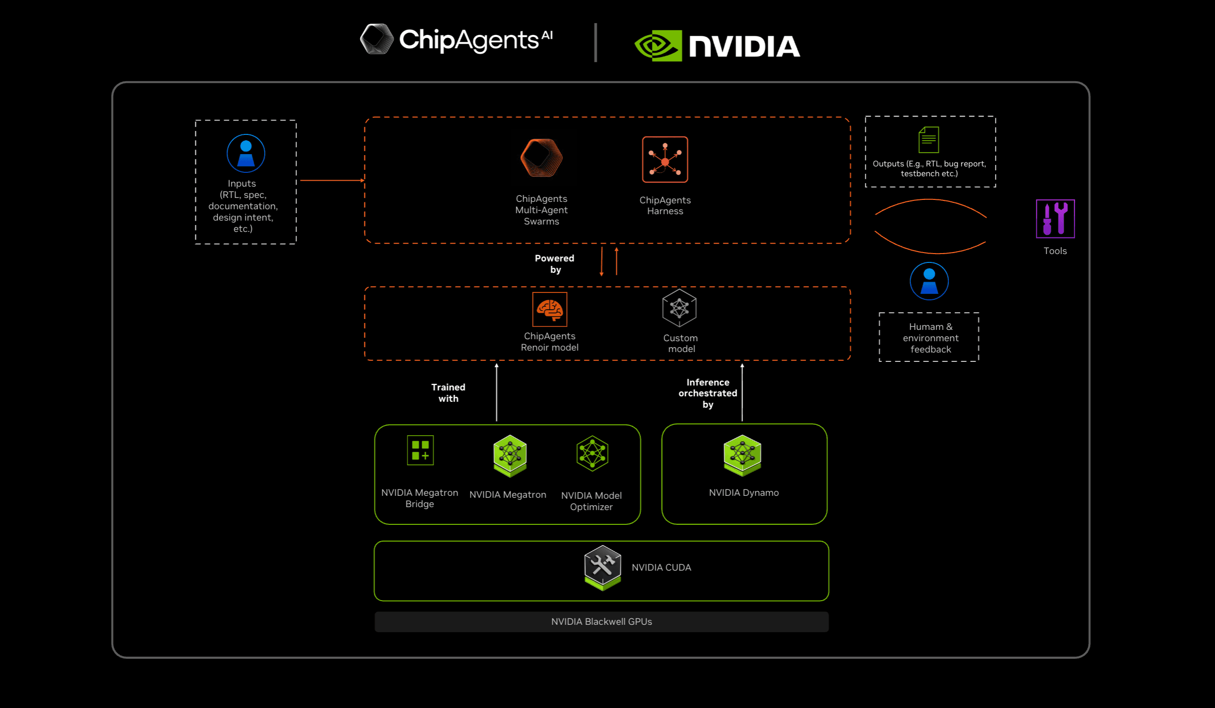
As seen in ChipAgents and NVIDIA's architecture, inputs such as RTL, specifications, documentation, and design intent can flow into ChipAgents' multi-agent swarms and harnesses. ChipAgents' Renoir model and custom models can be trained and powered using NVIDIA infrastructure including Megatron, Megatron Bridge, Model Optimizer, Dynamo, CUDA, and Blackwell GPUs. The agents can then interact with engineering tools and incorporate both human and environmental feedback to produce outputs such as RTL, bug reports, and testbenches.
The direction is toward an engineering environment where agents go beyond generating code to interact continuously with the complete semiconductor workflow.
They can reason over specifications and design intent, call trusted EDA tools, inspect simulation and verification evidence, incorporate physics, learn from previous iterations, and continue working toward measurable engineering objectives.
And as those underlying simulations become faster, AI physics models become more capable, and agentic frameworks become more sophisticated, the closed loop itself becomes faster.
That is what begins to move semiconductor engineering from AI-assisted design toward truly AI-native chip design—from physics to silicon.
Watch the Presentation: Karthik On-Demand