
Closed-Loop Autonomous Design: How Agentic AI Is Reshaping Semiconductor Engineering

Semiconductor design is experiencing an automation revolution.
From synthesis' transformation of RTL into gates, place-and-route automating physical implementation, and verification tools making it possible to reason across designs containing billions of transistors; the chip design industry has spent decades automating increasingly complex engineering tasks.
But, as chips have continued to grow in complexity, simply improving individual tools with AI features is no longer enough. Now, the more significant shift lies in full-flow automation.
This is where Agentic AI becomes essential.
As AI systems evolve from copilots that answer questions into autonomous agents capable of using tools, analyzing results, debugging failures, and collaborating with other agents, semiconductor engineers can begin delegating entire workflows rather than individual tasks.
In a recent Silicon Grapevine conversation with EE Times, ChipAgents Founder and CEO William Wang described this transition from AI-assisted engineering toward increasingly autonomous chip development. ChipAgents itself followed that trajectory: beginning with a single-agent system before moving toward multiple autonomous agents capable of executing complex workflows from end to end.
The Semiconductor Industry Has a Scaling Problem
With the rise of 3D IC chips and heterogeneous integration, chip design is becoming exponentially more complex. In contrast, the number of experienced engineers available to design and verify those chips is remaining relatively stagnant. Home-grown agentic workflows still depend heavily on manual work by engineers: navigating interfaces, inspecting results, and coordinating across highly specialized teams.
This model becomes increasingly difficult to scale as designs grow toward trillions of transistors. Simultaneously, the challenge moves beyond making engineers type RTL faster and becomes expanding the amount of engineering work each person can effectively oversee.
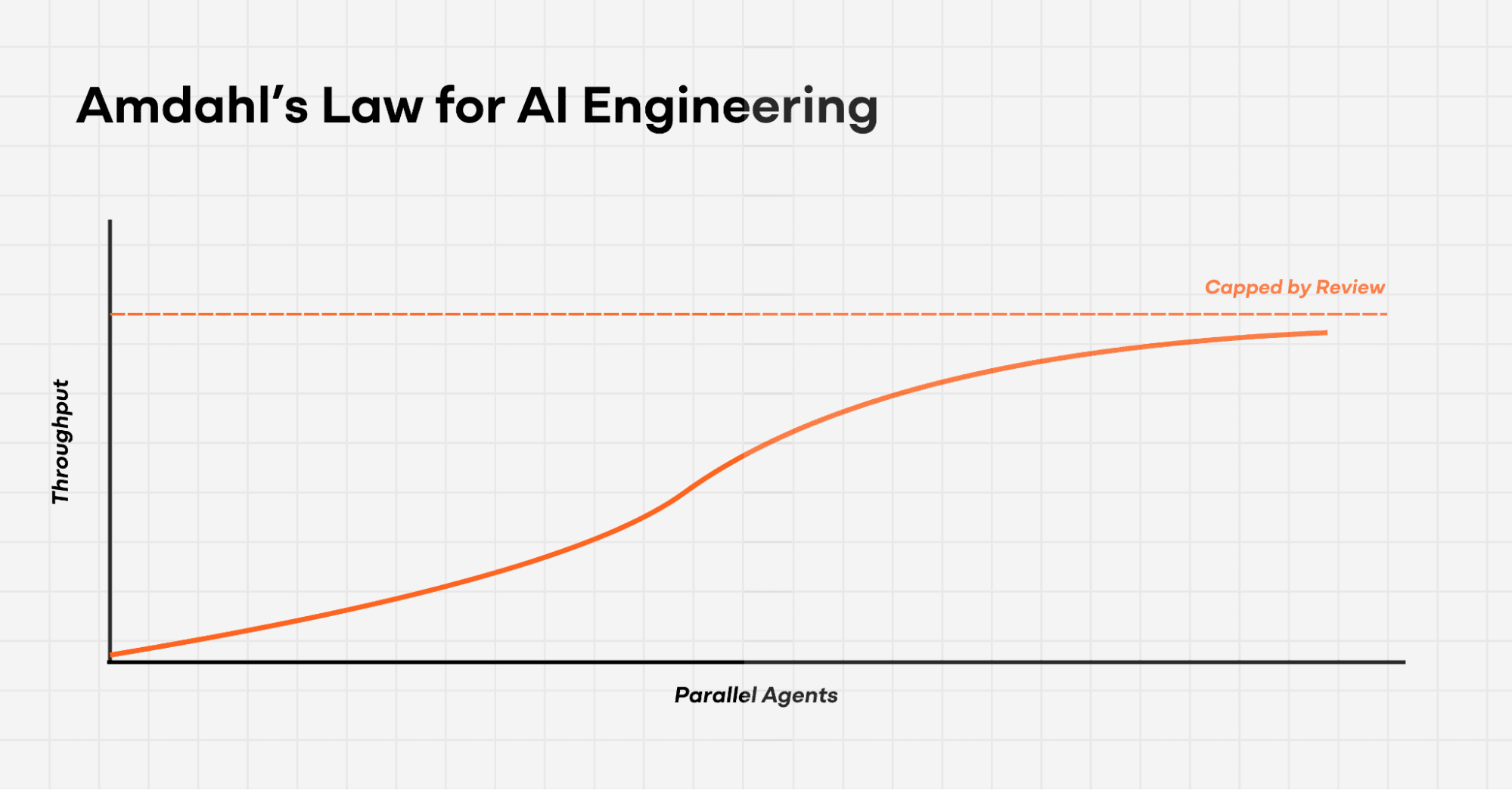
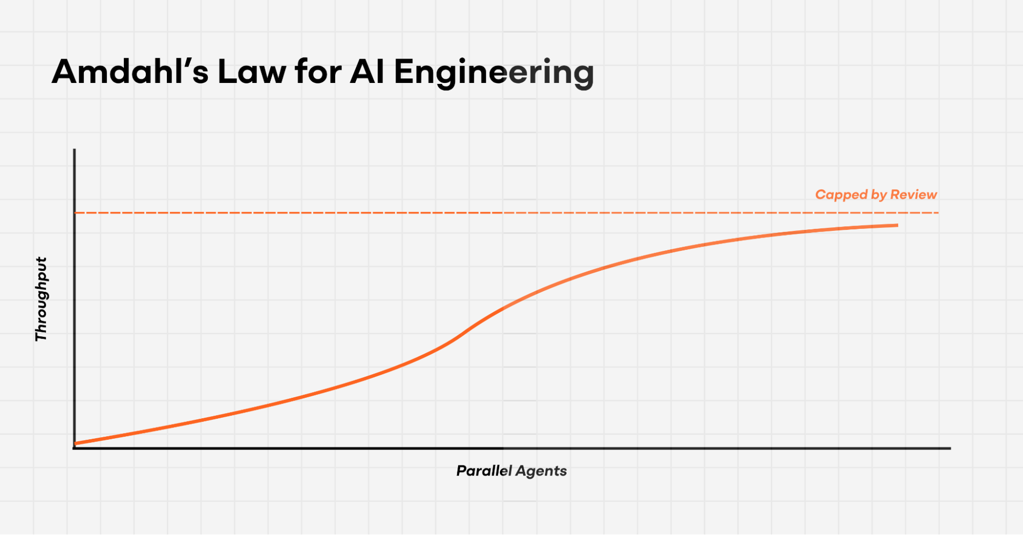
This creates an ‘Amdahl's Law’ for AI engineering: generation scales horizontally, while human review caps this growth. This bottleneck in the reviewing process explains the threat of engineering agents to be ‘almost right’.
AI itself lacks understanding of design know-how, data, and tool behaviors, consequentially wasting millions of tokens in its efforts to meet the standard of human review. By simply adding more singular agents into this process, compute, tooling, and inference costs are all driven up, while ROI diminishes. Worse than this, an almost right solution in silicon can easily become a mask set.
To properly scale using agentic AI, systems must be built to keep up with demand while also generating, evaluating, rejecting, and improving solutions without requiring a human to manually inspect every intermediate output.
Multi-Agent Engineering Mirrors How Chip Teams Already Work
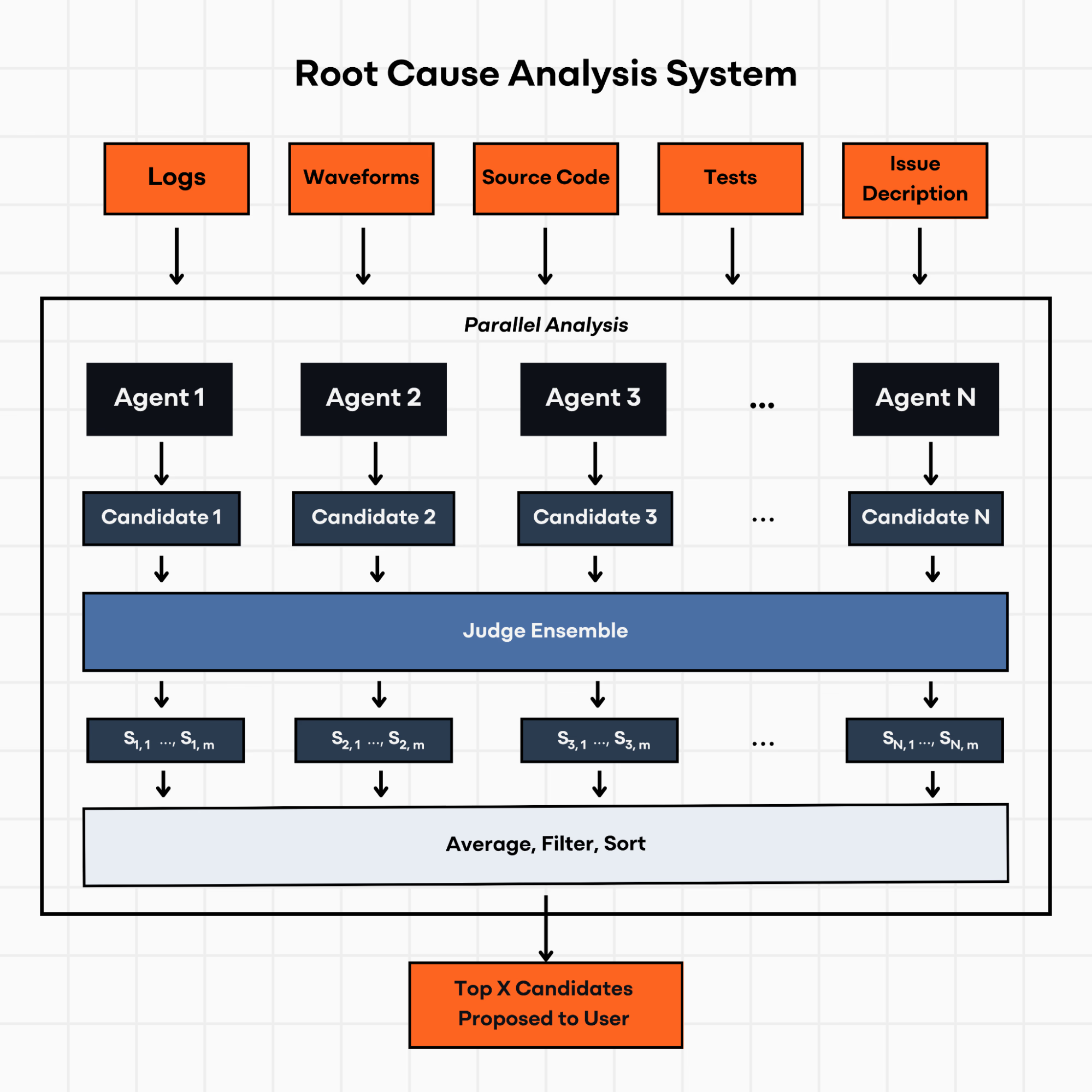
Today, difficult bugs often bring together architects, designers, verification engineers, and software engineers. Each person approaches failure from a different perspective. One engineer may inspect waveforms while another studies the RTL, logs, specification, or software behavior. Together, they form hypotheses, challenge one another's conclusions, and work backward toward the root cause.
A multi-agent system can begin to reproduce this structure computationally.
Similarly to the behavior of engineers, different agents can take on different roles: one inspecting waveform behavior, another analyzing logs, another examining the design, and others reasoning about specifications or potential failure mechanisms. Those agents can then combine their findings to isolate the relevant timestamp, identify the root cause, and trace the problem back toward the RTL.
This becomes especially important as SoCs expand across increasingly complex environments involving processors, memory, accelerators, and multiple chips. The volume of information involved is simply becoming too large for engineers to inspect manually at every stage.
Therefore, the long-term opportunity is not one AI assistant per engineer; it is one engineer orchestrating many specialized agents on an integrated platform.
Verification Is a Natural Starting Point
Full autonomous chip design will not arrive everywhere at once.
The most successful deployments are likely to begin with workflows where AI can create substantial value while its output remains measurable and verifiable.
Verification is particularly well suited to this model. Tasks such as functional verification, formal verification, test-plan generation, code review, auditing, and debugging already involve large amounts of repetitive analysis. More importantly, the goal is often to find something wrong rather than directly modify a production design.
By reframing the problem as a search for data, rather than pruning the data itself, agents are able to ask high level questions about various signals. Through a request for data, the agent is able to ask questions such as, “where does this signal diverge after the 10th packet is sent?”, and receive compact, symbolic answers to deliver back to the engineer. In simpler terms, the agents are able to simultaneously analyze components, trace failures to origin, and suggest fixes.
These factors make verification a relatively natural environment for building trust.
Instead of asking an AI system to generate RTL and immediately accepting its output, an engineering organization might first deploy agents to review existing code, search for bugs, generate verification collateral, or analyze failures. Engineers can compare those results against established workflows and expand usage as confidence grows.
From there, agentic workflows can move further upstream into specification analysis and spec-to-RTL generation, and downstream into physical design, manufacturing, and testing.
ChipAgents view is ultimately end-to-end: connecting these currently fragmented stages into increasingly autonomous engineering loops.
The Engineer's Job Moves Up a Level
Perhaps the most consequential change will be what engineers spend their time doing.
In the case of debugging: a verification engineer may spend hours navigating waveforms, searching through enormous numbers of signals, identifying the relevant timestamp, tracing behavior through the design, and eventually returning to the RTL.
With this new work flow, AI agents can absorb more of that investigative work.
In tradeoff, the engineer can spend more time deciding what should be tested, which failures matter, which architectural alternatives should be explored, and what the system should ultimately do.
This distinction becomes even more pronounced for experienced engineers.
A senior engineer with agents at their disposal no longer has to personally execute every investigation. Instead, they can dispatch different agents against different problems and evaluate their findings. Meanwhile, junior engineers can use the same systems to understand unfamiliar blocks, navigate legacy code, and learn established engineering practices faster.
In other words, AI has moved beyond making existing engineering tasks faster; it is now moving engineers from execution toward orchestration and decision-making.
Trust and Security Become Engineering Requirements
With greater autonomy also comes an understandably higher bar for trust.
Semiconductor design is fundamentally different from many consumer AI applications. A plausible answer is not sufficient when a mistake can propagate through months of engineering work and ultimately contribute to a failed tape-out.
Successful adoption therefore depends on choosing workflows where outputs can be checked, creating appropriate sandboxing and security boundaries, and gradually expanding autonomy as systems demonstrate reliability.
Data protection is equally important. For many semiconductor companies, design files, proprietary intellectual property, and internal debugging logs are too sensitive to be sent to third-party cloud environments. AI infrastructure therefore needs to fit within the industry's security requirements, including private deployment models and policies around customer data.
This core requirement for deploying agentic AI, emphasizing private cloud environments, sandboxing, security controls, and a policy of not training models on customer data is exemplified by Renoir, ChipAgents own LLM. Renoir enables AI models to run in an air-gapped, on-premises environment allowing teams to fully own their deployment, data, and security policies.
As agents become capable of taking more actions, safeguards like these become especially important. Autonomy without control is reckless, not useful engineering automation.
From Productivity Gains to Time-to-Market
A semiconductor company rarely has the luxury of simply extending a schedule because a design has become more complex. Engineering organizations are often managing multiple chips simultaneously against aggressive tape-out windows.
That means even relatively small improvements across specification analysis, RTL development, verification, debugging, and physical design can compound across an entire program.
Through ChipAgents implementation with Whalechip, an IC design company specializing in 3DIC and Wafer-on-Wafer (WoW) advanced packaging technology, these improvements were exemplified.
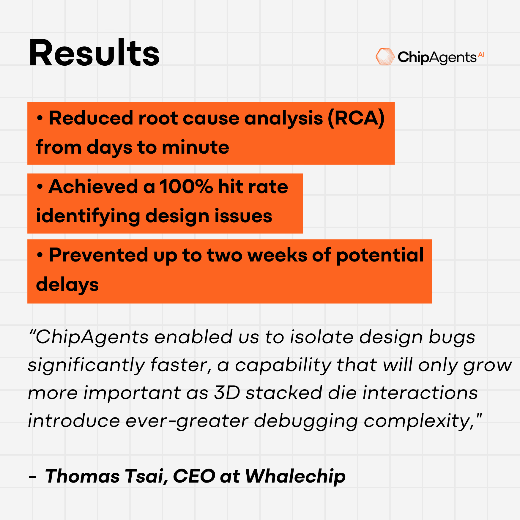
Using ChipAgents' agentic AI platform, Whalechip reduced root cause analysis from days to minutes, achieved a 100% hit rate on design issue identification, and prevented up to two weeks of potential delays.
There is an even larger opportunity that comes when these improvements stop being isolated.
By connecting agents across multiple stages, the possibility of continuous engineering loops in which systems generate, test, analyze, revise, and optimize, with humans supervising the higher-level objectives, becomes a reality.
Toward Autonomous Chip Development
Autonomy is more likely to expand incrementally. Individual workflows become autonomous first. Then adjacent workflows become connected. Verification may connect with physical design and physical verification. Front-end and back-end workflows may increasingly exchange information automatically. Eventually, manufacturing and testing can become part of the same broader system.
Connecting the entire front end, back end, manufacturing, and testing flow could still take three to five years. Even once we reach this point, humans remain central to deciding what should be built and making important engineering decisions. But, a much larger share of the execution itself could become autonomous.
That distinction may define the next era of semiconductor engineering.
Humans specify intent, architecture, constraints, and priorities while agents increasingly handle execution, exploration, analysis, and iteration.
Meaning, the engineer will not disappear from the design process; they move up a level.
As chip complexity continues to outpace the industry's ability to add engineering headcount, this shift may become less about adopting a new AI tool and more about creating the only practical way to scale semiconductor engineering itself.
Frequently Asked Questions
What is closed-loop autonomous chip design?
Closed-loop autonomous design is an approach where AI agents generate, test, analyze, revise, and optimize chip design work in continuous loops, with engineers supervising the higher-level objectives. ChipAgents founder and CEO William Wang discussed this shift from AI-assisted engineering toward increasingly autonomous chip development in a Silicon Grapevine conversation with EE Times.
Why is verification a natural starting point for autonomous chip design?
According to ChipAgents, verification outputs can be measured and checked, and the goal is often to find something wrong rather than to modify a production design. That lets teams deploy agents to review code, search for bugs, and analyze failures, compare the results against established workflows, and expand usage as confidence grows.
How long until fully autonomous chip design?
ChipAgents expects autonomy to expand incrementally, with individual workflows becoming autonomous first and adjacent workflows connecting over time. Connecting the full front-end, back-end, manufacturing, and testing flow could take three to five years, and humans will still decide what gets built.
How does ChipAgents keep autonomous AI secure?
ChipAgents emphasizes private deployment models, sandboxing, security controls, and a policy of not training models on customer data. Its Renoir model can run in an air-gapped, on-premises environment, so teams fully own their deployment, data, and security policies.
What results has closed-loop AI delivered in production?
Using ChipAgents' agentic AI platform, Whalechip, an IC design company specializing in 3DIC and wafer-on-wafer packaging, reduced root cause analysis from days to minutes, achieved a 100% hit rate on design issue identification, and prevented up to two weeks of potential delays.